Semicon India 2026: Rs13.5 Billion Semiconductor Mission Targets Global Self-Reliance
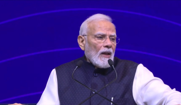
Prime Minister Narendra Modi inaugurated the fifth edition of Semicon India 2026 on September 17 at Yashobhoomi in New Delhi, announcing a $13.5 billion second phase of India's Semiconductor Mission targeting self-reliance in chip design, manufacturing, and packaging. The government confirmed that 12 semiconductor manufacturing projects have been approved, with 5 units already in commercial production and multiple others at various stages of implementation. The theme 'Silicon to Systems: Building the Ecosystem' reflects India's ambition to move beyond individual chip production to building end-to-end semiconductor value chains domestically. The three-day event attracted over 600 participating companies, 50,000 expected visitors, and representatives from 52 countries.
What did India announce at Semicon India 2026?
Inaugurating Semicon India 2026 in New Delhi on September 17, Prime Minister Modi announced a $13.5 billion second phase of the India Semiconductor Mission, which began in 2021 with ₹75,000 crore. Twelve chip projects have been approved and five are in commercial production. The theme, Silicon to Systems, signals a push from single fabs to a full domestic value chain.
India is becoming a preferred destination for semiconductor manufacturing. We are not just importing chips; we are building the ecosystem to design, manufacture, package, and export semiconductors globally.
PM Narendra Modi, Semicon India 2026, September 17, 2026
What Happened?
India's Semiconductor Mission, first launched in 2021 with an initial Rs75,000 crore allocation, is now entering its second phase with an additional $13.5 billion (approximately Rs1,13,000 crore). The mission covers five pillars: (1) Semiconductor fabrication (fabs), (2) Semiconductor assembly, testing, marking and packaging (ATMP), (3) Chip design, (4) Equipment and materials, and (5) Talent development. Currently, 12 major projects have been approved: Micron Technology (fab in Gujarat), ISMC (RIMC in Rajasthan), SK Hynix (assembly in Gujarat), and others. The government has streamlined regulatory processes and offered incentives including capital subsidies (up to 30% for fabs) and production-linked incentives (PLI) schemes. Five units have commenced commercial production, producing memory chips and semiconductor components for global markets.
India's semiconductor strategy reflects a shift from dependency to strategic autonomy. Historical context: India relied entirely on chip imports until 2021. The COVID-19 pandemic exposed this vulnerability when global chip shortages disrupted Indian manufacturing. Simultaneously, Western export controls on advanced chips to China signaled that semiconductor technology is a geopolitical weapon. India recognised that without domestic chip production, it would remain strategically vulnerable. The Semicon 2026 announcements show progress, but challenges remain: fab construction requires 4-5 years, achieving technological parity with Taiwan/South Korea takes a decade, and maintaining profitability in a cyclical industry is difficult. India's strategy focuses on specific segments (memory chips, automotive semiconductors, defence chips) where it can achieve competitiveness quickly rather than competing across the entire spectrum.
Why It Matters
Semiconductor self-reliance has three dimensions. First, economic: the global chip industry is worth $600 billion annually; India captures a fraction through software and design services. Controlling fabrication would capture value-addition. Second, strategic: modern weapons systems (radars, missiles, drones) depend on semiconductors. Countries without chip technology cannot build modern militaries. Third, geopolitical: semiconductor bottlenecks are leverage points. China has felt this acutely; India is learning the lesson. For UPSC, Semicon 2026 exemplifies how industrial policy, FDI attraction, and technology development converge to achieve strategic autonomy. It also tests understanding of comparative advantage: India excels in design and software but lags in manufacturing; the mission aims to close this gap.
Concept Behind the News: Semiconductor Supply Chains
- Fabless vs. fab-based: Most chip design companies (Qualcomm, MediaTek) don't manufacture; they license fabs (Taiwan TSMC, Samsung). India wants to own both design and fab.
- Fab economics: A modern fab costs $10-15 billion, takes 4-5 years to build, and operates continuously (not profitable if idle). High barriers to entry.
- ATMP (Assembly, Testing, Marking, Packaging): Lower-tech, lower-cost segment; easier for India to enter. Gives revenue before fabs mature.
- Chip design: India has strength here (through semiconductor design at IIT, startups). Can target AI chips, automotive semiconductors.
- Global supply chain: Taiwan (TSMC) controls 50%+ of global foundry capacity. South Korea (Samsung) follows. America relies on both. India's goal: 5-10% of global capacity by 2030.
- Strategic implications: Chip independence means not being held hostage by Taiwan or US export controls.
Syllabus Connection
- GS-III (Economy): FDI policy, industrial policy, Make in India, skill development
- GS-III (Science & Technology): Semiconductor technology, chip design, manufacturing capability
- GS-II (Government initiatives): Central schemes for technology development and manufacturing
PYQ Connection
UPSC Prelims 2025 — Financial Markets, FDI & Industrial Infrastructure
Question: Consider the following statements: Statement I: Interest income from deposits in Infrastructure Investment Trusts (InvITs) distributed to their unit-holders is taxable as income from other sources. Statement II: InvITs can be listed on stock exchanges. Which is correct?
- Only I is correct
- Only II is correct
- Both are correct
- Neither is correct
Answer: Both are correct
Both correct. InvITs are financial instruments attracting FDI for infrastructure projects like semiconductor facilities. Understanding InvITs is essential for understanding how India finances capital-intensive manufacturing projects.
Question: Which one of the following launched the 'Nature Solutions Finance Hub for Asia and the Pacific'?
- Asian Development Bank
- World Bank
- UNEP
- Regional Environmental Centre
Answer: Asian Development Bank
Multilateral institutions finance infrastructure development. Understanding international financing mechanisms helps contextualize India's semiconductor funding strategy and FDI attraction policies.
Question: Consider the following statements: The 'Stability and Growth Pact' of the European Union: 1. Limits budgetary deficit to 3% of GDP. 2. Restricts member states' FDI inflows. 3. Governs monetary coordination. Which is correct?
- Only 1
- 1 and 3 only
- 2 and 3 only
- All three
Answer: 1 and 3 only
Statements 1 and 3 are correct. Understanding international industrial policy frameworks helps contextualize India's fiscal strategy for semiconductor investment and FDI regulation.
CAPF 2020-2024 — Infrastructure, Manufacturing & Industrial Sector
Question: SAUBHAGYA, a Central Government scheme, is related to:
- Electricity distribution to rural areas
- Water infrastructure development
- Road construction
- Telecommunications expansion
Answer: Electricity distribution to rural areas
Electricity distribution is critical infrastructure for semiconductor fabrication facilities. Government infrastructure schemes enable manufacturing sector development by providing essential utilities.
Question: Which of the following are India's G20 priorities? 1. Green Development 2. Women-led Development 3. Climate Finance 4. Digital Public Infrastructure. Which is correct?
- Only 1 and 2
- Only 2 and 3
- Only 3 and 4
- All four
Answer: All four
All are correct. India's G20 presidency emphasizes digital infrastructure and climate-aligned manufacturing. Semiconductor manufacturing aligns with all four priorities.
Question: Which among the following are the main ingredients for manufacturing of glass?
- Silica, Soda Ash, Limestone
- Silica, Lime, Iron Oxide
- Silica, Feldspar, Quartz
- Silica, Potassium, Sodium
Answer: Silica, Soda Ash, Limestone
Silica-based materials are foundational to semiconductor wafer manufacturing. Understanding materials science is essential for understanding chip production processes and supply chains.
UPSC Mains 2013-2019 — FDI, Industrial Location & Strategic Policy
2013 | Investment Models: (a) Discuss the impact of FDI entry into Multi-trade retail sector on supply chain management in commodity trade pattern of the economy. (100 words) (b) Explain the role of FDI in India's industrial growth. Exam relevance: Understanding FDI's role in semiconductor manufacturing; how foreign capital and technology transfer drive industrial capability.
2013 | Infrastructure: Write a note on India's green energy corridor to alleviate the problem of conventional energy. Exam relevance: Power infrastructure required for semiconductor fabrication plants; India's renewable energy strategy supports fab construction.
2014 | Government Policies: Though 100% FDI is already allowed in non-news media like trade publications and entertainment channels, the government is mulling over allowing 100% FDI in news media. What are the possible benefits and challenges? Evaluate. Exam relevance: Understanding government's selective FDI policy—directly applicable to semiconductor sector where India restricts FDI in sensitive technologies.
2019 | Natural Resources & Industrial Location: Can the strategy of regional resource-based manufacturing help in promoting employment in India? Discuss with specific examples. Exam relevance: Distributing semiconductor manufacturing across Gujarat, Rajasthan, Karnataka creates employment; Semicon India reflects this regionalized strategy.
Visual Explanation: Global Foundry Capacity & India's Growth Trajectory
Global Semiconductor Foundry Capacity Distribution
| TSMC (Taiwan) | 51 |
|---|---|
| Samsung (S.Korea) | 17 |
| Intel (USA) | 8 |
| GlobalFoundries (USA) | 6 |
| UMC (Taiwan) | 10 |
| India (Target 2030) | 0.5 |
Fab vs ATMP Economics (Capital Requirements)
| Fab (Fabrication Plant) | 12 |
|---|---|
| ATMP (Assembly/Testing) | 2.5 |
| Design Center | 0.5 |
Connect the Dots
- 2020: COVID-19 exposes India's semiconductor import dependency; global chip shortage disrupts manufacturing
- 2021: Government launches Semiconductor Mission with Rs75,000 crore; targets domestic fab capacity
- 2022-2023: First approval of Micron, ISMC projects; construction begins
- 2024-2025: DRDO achieves GaN technology breakthroughs; shows domestic design capability
- September 2026: Semicon India 2026; Rs13.5B additional allocation; 5 units in production
- 2027-2030: Scale-up phase; India targets 5-10% of global semiconductor capacity
Read More
Read More
- India Semiconductor Mission Official (Government roadmap and approved projects)
- SEMI (Semiconductor Equipment and Materials International) (Global semiconductor industry body tracking India's progress)
Exam Takeaway
- Semiconductors are the new strategic resource; countries without chip technology are strategic dependencies
- India's strategy: focus on specific segments (memory, automotive) before competing globally across all chips
- FDI + PLI incentives are tools to attract global manufacturers; partnership model beats trying to build entirely domestically
- Fab construction timelines (4-5 years) mean decisions made today determine India's competitiveness in 2030
- Technology self-reliance requires long-term commitment, not just one-time investment
Exam Angle
For mains: write an essay on why semiconductor self-reliance is essential for India's strategic autonomy (defence, economy, geopolitics). For prelims: understand the semiconductor value chain—design, fab, packaging—and India's current strengths and weaknesses in each segment.
Possible Question
Question: India's Semiconductor Mission prioritises which of the following segments?
- Chip design only (fabless model)
- Chip design, fab manufacturing, ATMP, equipment, and talent development
- ATMP and packaging only
- Memory chip fabrication only
Answer: Chip design, fab manufacturing, ATMP, equipment, and talent development
The mission covers all five pillars of the semiconductor value chain: design, fabrication (fabs), assembly/testing/packaging (ATMP), equipment/materials, and talent development. This comprehensive approach aims to build an integrated ecosystem rather than relying on imports or single segments.
Sources & Further Reading
- Business Today: SEMICON India 2026 - PM Modi highlights $13.5B semiconductor mission (Sept 17, 2026)
- SEMI: PM to Inaugurate SEMICON India 2026 (Sept 17, 2026)
- ANI News: PM Modi visits SEMICON India 2026 exhibition (Sept 17, 2026)
- Indian Masterminds: From Chip Design to Global Manufacturing - PM Modi Sets Out India's Roadmap
- PIB: PM inaugurates SEMICON India 2026